3D printing has become a real game-changer in the modern world. It can make all sorts of objects and is not at the mercy of large production lines. At one point, someone could even 3D print food. Now, researchers funded by NASA will apply the technology and manufacturing methods to print sensors and even part of the circuitry used for wireless communication on a circuit board smaller than your phone.
According to the presentation, the multi-sensor platforms used by scientists on Earth and in space have traditionally been built like any electronic product today. Each different sensor was manufactured separately and then integrated with other components on a circuit board, a process that was not only painstaking but also subject to errors somewhere along the assembly line.
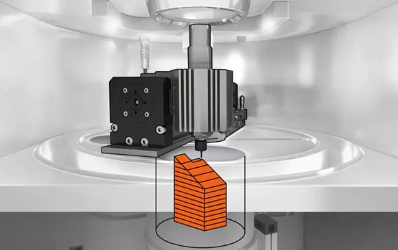
The 3D printing technology being investigated by Mahmooda Sultana and her team at NASA Goddard Space Flight Center will simplify the production and packaging of these important platforms. Using nanomaterials such as carbon nanotubes and graphene, they will print all the necessary sensors in a single process and on the same substrate. They could even 3D print parts of the wireless communication circuits that are necessary for the platform to communicate with the ground controller for data.
If Sultana and her team are successful, they could change the face of NASA research forever. Each platform will be self-sufficient, able to detect a variety of environmental data, from gas concentrations to atmospheric pressure to temperature, and transmit that data on its own. All that is needed is to add a power supply and communication circuitry to the rest. 3D printed multi-use sensor platforms not only simplify the production process, but also reduce power consumption and chip size, which in turn could be used not only on planetary rovers, but even on space suits to monitor health and safety.
In recent years, NASA has been at the forefront of adopting cutting-edge technologies to enhance space exploration and scientific advancements. One such groundbreaking innovation is the integration of sensors into silicon wafers using 3D printing technology. This revolutionary approach has opened up new avenues for space missions, making them more efficient, cost-effective, and reliable. In this blog post, we will delve into the exciting world of 3D-printed sensors in silicon wafers and explore how this game-changing technique is propelling NASA’s missions to greater heights.
1. The Marriage of 3D Printing and Silicon Wafers
Silicon wafers have long been a crucial component in the semiconductor industry, serving as a substrate for electronic devices like microprocessors and sensors. Combining 3D printing with silicon wafers allows NASA to fabricate intricate and custom sensor designs directly onto the wafer’s surface. This marriage of technologies presents a host of advantages, including reduced production costs, enhanced sensor performance, and improved mission flexibility.
2. Advantages of 3D-Printed Sensors in Silicon Wafers
- Reduced Weight and Size: Traditional sensor integration involves multiple components, leading to added weight and bulkiness. With 3D printing, sensors can be integrated directly onto the silicon wafer, eliminating the need for extra components and reducing the overall weight and size of the system.
- Enhanced Sensor Performance: Precise 3D printing techniques enable the creation of complex sensor structures that enhance sensitivity, accuracy, and reliability. This advancement is critical in gathering accurate data from harsh and challenging space environments.
- Cost-Effectiveness: Integrating sensors through 3D printing streamlines the manufacturing process, reducing production costs. Additionally, 3D printing allows rapid prototyping, saving time and resources during the development phase.
3. Applications in Space Exploration
- Robotic Missions: 3D-printed sensors play a pivotal role in robotic missions, enabling autonomous navigation, obstacle avoidance, and data collection. These sensors can be customized to suit the specific requirements of each mission, optimizing their performance.
- Environmental Monitoring: Integrating sensors into silicon wafers enhances NASA’s ability to monitor and understand the environment in space and on other celestial bodies. This data is crucial for studying space weather, planetary atmospheres, and geological features.
- Human Spaceflight: For human missions, 3D-printed sensors can be employed for various applications, such as monitoring astronauts’ health, ensuring life support systems’ functionality, and assisting with spacewalk activities.
4. Future Prospects and Challenges
The integration of sensors into silicon wafers using 3D printing marks a significant milestone for NASA. However, some challenges lie ahead:
- Material Compatibility: Identifying and using suitable materials that can withstand the harsh conditions of space is vital for long-term sensor reliability.
- Testing and Validation: Rigorous testing and validation processes are necessary to ensure the sensors perform as expected in space environments.
- Scalability: As the demand for advanced sensors grows, ensuring the scalability of 3D printing technologies becomes crucial to meet future mission requirements.
- Interdisciplinary Collaboration: Successful implementation of 3D-printed sensors requires collaboration between experts in 3D printing, materials science, and space exploration.
Related Questions and Answers
Q1: How does 3D printing benefit sensor integration in silicon wafers?
A1: 3D printing allows the fabrication of custom and intricate sensor designs directly onto the silicon wafer’s surface, reducing weight, enhancing performance, and streamlining production, thus making the integration process more efficient.
Q2: What are the applications of 3D-printed sensors in space exploration?
A2: 3D-printed sensors find applications in robotic missions for autonomous navigation, obstacle avoidance, and data collection. They are also used for environmental monitoring and human spaceflight, aiding in health monitoring and life support systems.
Q3: What challenges does NASA face with 3D-printed sensor integration?
A3: NASA faces challenges related to material compatibility, rigorous testing, scalability, and the need for interdisciplinary collaboration to ensure successful implementation of 3D-printed sensors in space missions.
Q4: How does the integration of sensors into silicon wafers benefit future space missions?
A4: This integration results in lighter and smaller sensor systems, improved performance, and cost-effectiveness, enabling NASA to gather more accurate data, enhance space missions, and pave the way for future explorations.
Conclusion
NASA’s pioneering use of 3D printing technology to integrate sensors into silicon wafers marks a turning point in space exploration. The advantages of this revolutionary approach are far-reaching, empowering NASA to conduct more efficient and cost-effective missions with improved sensor performance. As technology continues to advance, we can expect even more exciting applications and discoveries, propelling us towards a better understanding of the cosmos.